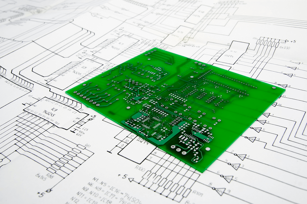
Schematic capture: This is the process of creating an electronic circuit diagram that represents the components and connections of the circuit.
Component placement: Once the schematic is created, components are placed on the board in their respective locations.
Routing: After components are placed, the connections between them are established by routing tracks, also known as traces, on the board.
Design rule check (DRC): This step ensures that the board design adheres to certain design rules and specifications.
Gerber file generation: Gerber files are generated from the PCB design, which contains all the information required to manufacture the board.
PCB fabrication and assembly: After the design is finalized, the PCB is fabricated and assembled with the necessary components.
Testing: The completed PCB is tested to ensure that it functions properly.
PCB design requires expertise in electronic circuits, software tools for schematic capture and board layout, and a good understanding of manufacturing processes.
It is important to follow industry standards and best practices to ensure that the design is functional, reliable, and cost-effective.
IPC (Institute for Printed Circuits) is an industry association that sets standards and guidelines for the design, manufacturing, and testing of printed circuit boards (PCBs). The IPC has developed a series of standards known as the IPC-A-600, IPC-A-610, and IPC-6012, which are used in the PCB industry to classify the quality and reliability of PCBs.
Class 1: Class 1 PCBs are used in products where cosmetic requirements are not important, and where the board is not subjected to harsh environments or extreme temperatures. Examples of products that use Class 1 PCBs include toys and consumer electronics.
Class 2: Class 2 PCBs are used in products where performance and reliability are important, but where the board is not subjected to extreme conditions. Examples of products that use Class 2 PCBs include computers, automotive systems, and industrial controls.
Class 3: Class 3 PCBs are used in products where high reliability is critical, and where the board is subjected to harsh environments or extreme temperatures. Examples of products that use Class 3 PCBs include aerospace and defense systems, medical devices, and telecommunications equipment.
The standards define specific requirements for each class of PCB, including criteria for things like plating thickness, solderability, and surface finish. PCB manufacturers and assemblers use these standards to ensure that their products meet the required level of quality and reliability for their intended use.
It is important for PCB designers and manufacturers to understand the different classes of PCBs and the requirements associated with each class in order to ensure that their products meet the necessary quality and reliability standards.
Design: The first step in PCB manufacturing is to design the board using specialized software. The design includes the placement of components, routing of traces, and other design features. Once the design is complete, it is saved as a computer file and prepared for manufacturing.
Material selection: The next step is to select the appropriate materials for the PCB, such as the substrate material, copper foil, and solder mask.
Film generation: The next step is to generate a film of the design. This involves printing the design onto a transparent film using a specialized printer. The film is then used to create the photomask, which is used to transfer the design onto the PCB.
Inner layer processing: For multilayer PCBs, the next step is to process the inner layers. This involves cleaning and preparing the copper-clad substrate, applying a photosensitive layer, and then exposing the photosensitive layer to the photomask using UV light. The exposed areas are then developed and the unexposed areas are etched away to create the copper traces and pads.
Outer layer processing: next step is to process the outer layers of the PCB. This involves applying a photosensitive layer to the substrate, exposing it to the photomask, and then developing and etching away the unexposed areas. This creates the outer layer traces and pads. In sort The circuit layout is etched onto the copper layers using a chemical process, leaving the desired traces and connections.
Drilling: Once the layers are processed, the next step is to drill holes for vias and through-hole components. The holes are drilled using specialized drilling machines and are then plated with copper to create electrical connections between the layers.
Plating: After the holes are drilled, the next step is to electroplate the entire surface of the board with a thin layer of copper. This creates a uniform surface that will be used for the final finish of the board.
Soldermask and silk screen: A solder mask is applied to the surface of the board to protect it from oxidation and to prevent solder from flowing into unwanted areas.Once the plating is complete, a soldermask is applied to the surface of the board to protect the copper traces and pads from damage during assembly. A silk screen layer is also added to provide labeling and other markings on the board.
Surface finish: The final step in PCB manufacturing is to apply a surface finish to the board. This can be done using a variety of methods, including immersion gold, immersion tin, and HASL (hot air solder leveling).
Quality control: Once the PCB is manufactured, it undergoes a series of quality control tests to ensure that it meets the required standards and specifications.
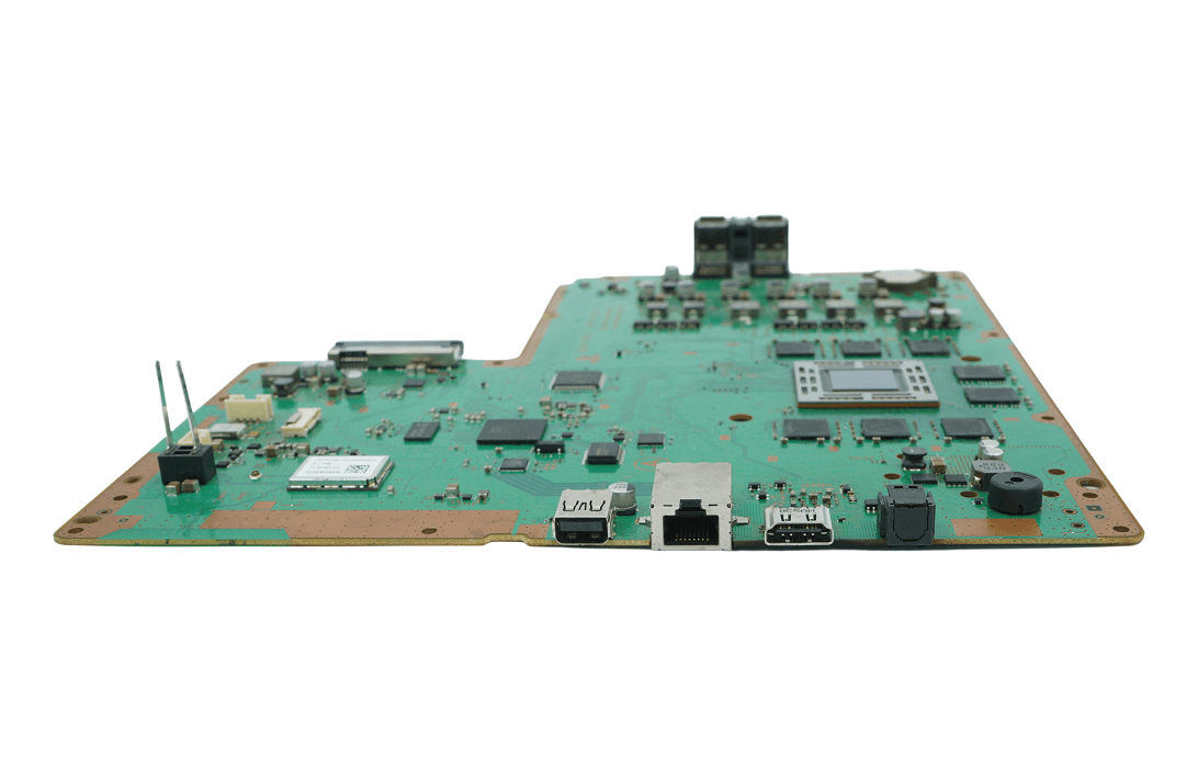
Assembly: After the PCB is manufactured, it can be assembled with the necessary components to create a functional electronic device.
Solder paste application: Solder paste is applied to the pads of the PCB using a stencil or a dispenser. The solder paste is a mixture of tiny balls of solder and flux, which acts as a temporary adhesive for the components.
Component placement: After the solder paste is applied, components are placed on the PCB, either by hand or by using automated pick-and-place machines. These machines can place components accurately and quickly, increasing the speed and precision of the assembly process.
Reflow soldering: Once the components are placed on the board, the PCB is passed through a reflow oven, which melts the solder paste and bonds the components to the board. During the reflow process, the solder paste flows to form a permanent connection between the components and the board.
Inspection: After the soldering process is complete, the PCB undergoes inspection to ensure that all components are properly soldered and in the correct location. Automated optical inspection (AOI) and X-ray inspection are commonly used for this purpose.
Testing: The completed PCB is tested to ensure that it functions properly. The test process can include functional testing, electrical testing, and other forms of testing to verify that the PCB meets the required standards and specifications.
Through-hole assembly: In this type of assembly, electronic components are inserted into pre-drilled holes on the PCB and then soldered onto the board. Through-hole assembly is a relatively simple and inexpensive process that is suitable for large, bulky components that require more physical support than surface mount components. However, it is not suitable for smaller, more complex components, which are typically used in modern electronic devices.
Surface mount assembly: In this type of assembly, electronic components are placed directly onto the surface of the PCB, rather than being inserted into pre-drilled holes. Surface mount components are typically smaller and more complex than through-hole components, and they can be placed onto the board using automated pick-and-place machines. Surface mount assembly is a more efficient and cost-effective process than through-hole assembly, and it is suitable for modern electronic devices that require smaller, more compact components.
Mixed assembly: In this type of assembly, both through-hole and surface mount components are used on the same PCB. This is often done when through-hole components are required for specific functions, or when surface mount components are not suitable for certain parts of the design. Mixed assembly requires additional steps to assemble the through-hole components, but it can offer a balance between cost, efficiency, and functionality.
Enclosure assembly: Once the PCB is tested and verified, it can be assembled into the final enclosure or housing. This may involve additional steps such as wiring, final assembly, and testing.
PCB assembly requires specialized equipment and expertise, and the process can vary depending on the complexity and size of the board. It is important to follow industry standards and best practices to ensure that the final product is functional, reliable, and cost-effective.