Starting from the idea of a product up to its realization, respecting your needs and managing the processing phases you need.
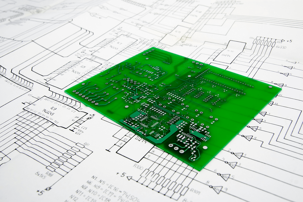
EVA PCB designs PCBs for every field, relying upon dedicated and up to date software's.
With an eye on quality, our team have worked with some of the leading companies on projects of all sizes.
Good design is like a refrigerator—when it works, no one notices, but when it doesn't, it sure stinks.
We'll start with an initial consultation, where you tell us what you need and we give you our thoughts on the project. After that, we can provide a quote and estimated timescales.
At EVA PCB, we prioritize customer satisfaction. We are dedicated to providing the best possible service and support for all your PCB design needs. Our highly professional and responsive team is always available to discuss your project and assist you throughout the design process.
PCB design is a complex process that requires a combination of technical expertise, design experience, and specialized tools. Our PCB design capability includes:
You may also receive additional files, such as assembly instructions, test procedures, and schematics, depending on your specific needs.
If you are interested in working with us on a project, please feel free to reach out to us. We would love to hear from you and discuss how we can help make your project successful.
You can send RFQs to the Sales e-mail address indicated in the Contact us page.
For securely transfer your large data files, Please contact our Sales Agents for your private FTP account. Alternatively, you can Email the entire package to our Sales Team.
Call Us Now